Popular Posts

New Posts

The nanoparticles are materials which size is in range from 1 to 100 nm \(\left(1 \left[\mathrm{nm}\right] = 1\times 10^{-9} \left[\mathrm{m}\right]\right)\). Depending on the shape they can be zero-dimensional (0D), one-dimensional (1D), two-dimensional (2D), and three-dimensional (3D). Based on their properties, sizes and shapes they can be classified to carbon based nanoparticles, metal NPs, Ceramics NPs, semiconductor NPs, polymeric NPs, and lipid-based NPs.

The carbon-based nanoparticles are fullerenes (0D NPs), carbon nanotubes (CNTs) (1D NPs), graphene sheets (2D NPs). Fullerenes gained interest from the industry due to their phenomenal properties such as electrical conductivity, mechanical strength, and elasticity, etc. CNTs due to their amazing properties are used in nanocomposites as fillers, efficient gas adsorbents, and support medium for different inorganic and organic catalysis. The graphene sheets proved as great NPs for capturing various gas molecules so possible implementation of these NPs could be as building blocks of extremely sensitive nanosensors in near future.

The metal NPs of the alkali and noble metals (Cu, Ag, and Au) have a broad absorption band in the visible zone of the electromagnetic solar spectrum. Gold NPs are used in the scanning electron microscope (SEM) to enhance the electronic stream which results in high-quality SEM images. Ceramic NPs are inorganic nonmetallic solids found in amorphous, polycrystalline, dense, and porous and hollow forms.

Semiconductor NPs have wide bandgaps and showed significant alteration in their properties with bandgap tuning. These materials are very important in photocatalysis, photo optics, and electron devices. Polymeric NPs are organic-based NPs that are in form of a sphere or a capsule. Lipid-based NPs is the largest spherical NPs with diameters in the range from 100 to 1000 nm. These NPs consist of a solid lipid core and soluble lipophilic molecules confined in a matrix. These NPs are one of the NPs used in applications such as drug carries and delivery and RNA release in cancer therapy.

There are various methods that can be used to synthesize NPs and they can be divided into the bottom-up approach and top-down approach. The bottom-up synthesis includes spinning, template support synthesis, plasma or flame spraying synthesis, laser pyrolysis, chemical vapor deposition (CVD) and atomic/molecular condensation. There is also some research conducted in the field of bottom-up biological synthesis using bacteria, yeasts, fungi, algae, and etc. On the other hand, top-down synthesis includes mechanical milling, chemical etching, sputtering, laser ablation, and electro-explosion.

The continuous investigation of NP materials has shown they possess extraordinary properties and due to these properties, there were some applications in drugs and medications, manufacturing and materials, environment, electronics, energy harvesting, and mechanical engineering. The NPs have been applied for drug delivery to increase drug therapeutic efficiency, weaken side effects, and improve patient compliance. Polyethylene oxide (PEO) and polylactic acid (PLA) NPs are promising systems for intravenous drug administration. Unique plasmon absorbance features of the noble metals NPs have been utilized in chemical sensors and bio sensors.

For more information about NPs check the article.

What are nanoparticles?

The nanoparticles are materials which size is in range from 1 to 100 nm \(\left(1 \left[\mathrm{nm}\right] = 1\times 10^{-9} \left[\mathrm{m}\right]\right)\). Depending on the shape they can be zero-dimensional (0D), one-dimensional (1D), two-dimensional (2D), and three-dimensional (3D). Based on their properties, sizes and shapes they can be classified to carbon based nanoparticles, metal NPs, Ceramics NPs, semiconductor NPs, polymeric NPs, and lipid-based NPs.

The carbon-based nanoparticles are fullerenes (0D NPs), carbon nanotubes (CNTs) (1D NPs), graphene sheets (2D NPs). Fullerenes gained interest from the industry due to their phenomenal properties such as electrical conductivity, mechanical strength, and elasticity, etc. CNTs due to their amazing properties are used in nanocomposites as fillers, efficient gas adsorbents, and support medium for different inorganic and organic catalysis. The graphene sheets proved as great NPs for capturing various gas molecules so possible implementation of these NPs could be as building blocks of extremely sensitive nanosensors in near future.

The metal NPs of the alkali and noble metals (Cu, Ag, and Au) have a broad absorption band in the visible zone of the electromagnetic solar spectrum. Gold NPs are used in the scanning electron microscope (SEM) to enhance the electronic stream which results in high-quality SEM images. Ceramic NPs are inorganic nonmetallic solids found in amorphous, polycrystalline, dense, and porous and hollow forms.

Semiconductor NPs have wide bandgaps and showed significant alteration in their properties with bandgap tuning. These materials are very important in photocatalysis, photo optics, and electron devices. Polymeric NPs are organic-based NPs that are in form of a sphere or a capsule. Lipid-based NPs is the largest spherical NPs with diameters in the range from 100 to 1000 nm. These NPs consist of a solid lipid core and soluble lipophilic molecules confined in a matrix. These NPs are one of the NPs used in applications such as drug carries and delivery and RNA release in cancer therapy.

There are various methods that can be used to synthesize NPs and they can be divided into the bottom-up approach and top-down approach. The bottom-up synthesis includes spinning, template support synthesis, plasma or flame spraying synthesis, laser pyrolysis, chemical vapor deposition (CVD) and atomic/molecular condensation. There is also some research conducted in the field of bottom-up biological synthesis using bacteria, yeasts, fungi, algae, and etc. On the other hand, top-down synthesis includes mechanical milling, chemical etching, sputtering, laser ablation, and electro-explosion.

The continuous investigation of NP materials has shown they possess extraordinary properties and due to these properties, there were some applications in drugs and medications, manufacturing and materials, environment, electronics, energy harvesting, and mechanical engineering. The NPs have been applied for drug delivery to increase drug therapeutic efficiency, weaken side effects, and improve patient compliance. Polyethylene oxide (PEO) and polylactic acid (PLA) NPs are promising systems for intravenous drug administration. Unique plasmon absorbance features of the noble metals NPs have been utilized in chemical sensors and bio sensors.

For more information about NPs check the article.


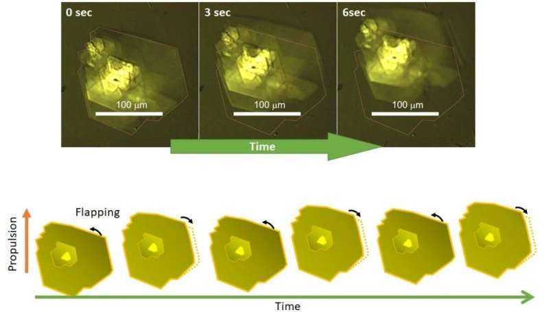
According to the research recently published in the journal Small, molecular mobile robots can swim in the water. The team from Hokkaido University led by Assistant Professor Yoshiyuki Kageyama had successfully created a microcrystal that utilizes self-continuous reciprocating motion for self-propulsion.
Figure 1 – a series of micrographs showing the movement of one of the synthesized microrobots in the study.
One of the key aspects of the microrobots and until recently one of the major challenges is self-propulsion or in other words the ability to move self-sustainably. To achieve the self-sustainable movement two major challenges had to be solved i.e. creation of a molecular robot that can reciprocally deform, and the ability to convert this deformation into propulsion of the molecular robot.
The Kageyama research team solved the self-propulsion problem of the molecular robot by confining the motion in two dimensions. In this system, the viscous resistance acts anisotropically which makes it negligibly weak. This molecular mobile robot is powered by blue light which drove a series of reactions and this leads to fin flipping and the propulsion. However, this motion is not continuous and occurs intermittently. The microrobot exhibit one of three different propulsion styles and these are: stroke, kick and side-stroke style. The mobility of a microrobot was affected by the area of the fin and its angle of elevation.
The computational minimum model was created in order to better understand the variables that affect the propulsion in the two-dimensional tank. The investigation showed that fin length, fin ratio, and elevation angle are the key variables that affect the direction and and pace of propulsion. The conducted investigation showed that tiny flippers can swim assisted by the anisotropy caused by confined spaces.
For more information check the full-length article: Obara, K., Kageyama, Y.,; Takeda, S. (2021). Self‐Propulsion of a Light‐Powered Microscopic Crystalline Flapper in Water. Small, 2105302.

Can molecular mobile robots swim in water?

According to the research recently published in the journal Small, molecular mobile robots can swim in the water. The team from Hokkaido University led by Assistant Professor Yoshiyuki Kageyama had successfully created a microcrystal that utilizes self-continuous reciprocating motion for self-propulsion.
Figure 1 – a series of micrographs showing the movement of one of the synthesized microrobots in the study.
One of the key aspects of the microrobots and until recently one of the major challenges is self-propulsion or in other words the ability to move self-sustainably. To achieve the self-sustainable movement two major challenges had to be solved i.e. creation of a molecular robot that can reciprocally deform, and the ability to convert this deformation into propulsion of the molecular robot.
The Kageyama research team solved the self-propulsion problem of the molecular robot by confining the motion in two dimensions. In this system, the viscous resistance acts anisotropically which makes it negligibly weak. This molecular mobile robot is powered by blue light which drove a series of reactions and this leads to fin flipping and the propulsion. However, this motion is not continuous and occurs intermittently. The microrobot exhibit one of three different propulsion styles and these are: stroke, kick and side-stroke style. The mobility of a microrobot was affected by the area of the fin and its angle of elevation.
The computational minimum model was created in order to better understand the variables that affect the propulsion in the two-dimensional tank. The investigation showed that fin length, fin ratio, and elevation angle are the key variables that affect the direction and and pace of propulsion. The conducted investigation showed that tiny flippers can swim assisted by the anisotropy caused by confined spaces.
For more information check the full-length article: Obara, K., Kageyama, Y.,; Takeda, S. (2021). Self‐Propulsion of a Light‐Powered Microscopic Crystalline Flapper in Water. Small, 2105302.


A new, flat lens with the ability to focus light with a higher efficiency within the visible spectrum was reported by a team of researchers from the Harvard John A. Paulson School of Engineering and Applied Sciences (SEAS) last summer. In order to bend and focus light as it passed, an ultrathin array of nanopillars was used in the lens.
The report was acknowledged as a major advancement in the field of optics and was mentioned as one of the Science Magazine’s top discoveries in the year 2016.However, one drawback in the lens was that it could focus only one color at a time.At present, the same team has produced the first flat lens with the ability to function within a continual bandwidth of colors, i.e. from blue to green. While being close to the bandwidth of an LED, this bandwidth opens the door for new applications in spectroscopy, imaging, and sensing.The study has been published in Nano Letters.One main problem faced by researchers developing a flat, broadband lens is correcting for chromatic dispersion, or the phenomenon in which different wavelengths of light get focused at different distances from the lens.

Therefore, in optics, it is highly significant to correct for chromatic dispersion, i.e. performing dispersion engineering, which is an important design requisite in any optical system dealing with light of different colors. The capacity of controlling the chromatic dispersion in flat lenses expands their implementation and makes way for new applications that are not practicable till date.In an attempt to initiate the commercialization of this technology by setting up a startup company, Harvard’s Office of Technology Development has filed patent applications on a portfolio of flat lens technologies and is working in collaboration with Capasso as well as researchers in his team.Alexander Zhu, Wei Ting Chen, Vyshakh Sanjeev, and Aun Zaidi coauthored the published study. The research was partially supported by the Air Force Office of Scientific Research. This research was carried out in part at Harvard University’s Center for Nanoscale Systems (CNS)—a member of the National Nanotechnology Coordinated Infrastructure (NNCI), in turn supported by the National Science Foundation.

Achromatic Flat Lenses Add More Color to the World of Optics


A new, flat lens with the ability to focus light with a higher efficiency within the visible spectrum was reported by a team of researchers from the Harvard John A. Paulson School of Engineering and Applied Sciences (SEAS) last summer. In order to bend and focus light as it passed, an ultrathin array of nanopillars was used in the lens.
The report was acknowledged as a major advancement in the field of optics and was mentioned as one of the Science Magazine’s top discoveries in the year 2016.However, one drawback in the lens was that it could focus only one color at a time.At present, the same team has produced the first flat lens with the ability to function within a continual bandwidth of colors, i.e. from blue to green. While being close to the bandwidth of an LED, this bandwidth opens the door for new applications in spectroscopy, imaging, and sensing.The study has been published in Nano Letters.One main problem faced by researchers developing a flat, broadband lens is correcting for chromatic dispersion, or the phenomenon in which different wavelengths of light get focused at different distances from the lens.

Therefore, in optics, it is highly significant to correct for chromatic dispersion, i.e. performing dispersion engineering, which is an important design requisite in any optical system dealing with light of different colors. The capacity of controlling the chromatic dispersion in flat lenses expands their implementation and makes way for new applications that are not practicable till date.In an attempt to initiate the commercialization of this technology by setting up a startup company, Harvard’s Office of Technology Development has filed patent applications on a portfolio of flat lens technologies and is working in collaboration with Capasso as well as researchers in his team.Alexander Zhu, Wei Ting Chen, Vyshakh Sanjeev, and Aun Zaidi coauthored the published study. The research was partially supported by the Air Force Office of Scientific Research. This research was carried out in part at Harvard University’s Center for Nanoscale Systems (CNS)—a member of the National Nanotechnology Coordinated Infrastructure (NNCI), in turn supported by the National Science Foundation.


Since the discovery of Carbon nanotubes made in 1991 scientists have tried to harness the unique properties of carbon nanotubes.  Some of them are calling it the material of 21. Century because of its extraordinary mechanical, electrical and thermal characteristics. The idea was to create high performance electronics that is faster and consume less power. Of course there was a number of challenges along the way and so far the silicon and gallium arsenide semiconductors outperformed carbon nanotube transistor. Just F.Y.I. the silicon and gallium arsenide semiconductors are used in computer chips.
The team from University of Wisconsin-Madison materials created carbon nanotube transistor that outperform conventional, latest silicon transistors. The team led by Michael Arnold and Padma Gopalan achieved current in carbon nanotube transistor that is 1.9 times higher than silicon transistors. Their discovery was published in journal Science Advances on September 2nd 2016.
Carbon nanotube transistor should replace silicon transistors and continue delivering the performance gains in computer industry. Carbon nanotube transistors should be able to perform five times faster or use five times less energy than silicon transistors according to research done so far.
The problem in creating this type of transistor was to isolate purely carbon nanotubes and they are crucial because metallic impurities act like copper wires and disrupt semiconducting properties. The research team used polymers to selectively sort out the semiconducting nanotubes and in this way they got carbon nanotubes with ultra-high-purity. To be more specific with this method the team have created carbon nanotubes with 0.01 % metallic impurities.
The other challenge in this research was placement and alignment of the nanotubes and that was very difficult to control. In order to make transistor CNT-s or carbon nanotubes have to be aligned in right order with just the right spacing when assembled on wafer. Of course the same team found the method to do so in 2014 called floating evaporative self-assembly.
Since they’ve used the polymer to isolate nanotubes this polymer acted as insulating layer between the nanotubes and the electrodes. To remove the polymer from CNT they’ve baked the nanotube arrays using vacuum oven to remove them. The result was excellent electrical contacts to nanotubes.
To validate extraordinary performance they benchmarked it against a silicon transistor of same size. So it’s finally here the point where researchers can exploit the nanotubes and nanostructures in general to attain performance gains in actual technology.


For more information about this cool new technology check out the Science Advances, DOI: 10.1126/sciadv.1601240 

Carbon nanotubes as transistors


Since the discovery of Carbon nanotubes made in 1991 scientists have tried to harness the unique properties of carbon nanotubes.  Some of them are calling it the material of 21. Century because of its extraordinary mechanical, electrical and thermal characteristics. The idea was to create high performance electronics that is faster and consume less power. Of course there was a number of challenges along the way and so far the silicon and gallium arsenide semiconductors outperformed carbon nanotube transistor. Just F.Y.I. the silicon and gallium arsenide semiconductors are used in computer chips.
The team from University of Wisconsin-Madison materials created carbon nanotube transistor that outperform conventional, latest silicon transistors. The team led by Michael Arnold and Padma Gopalan achieved current in carbon nanotube transistor that is 1.9 times higher than silicon transistors. Their discovery was published in journal Science Advances on September 2nd 2016.
Carbon nanotube transistor should replace silicon transistors and continue delivering the performance gains in computer industry. Carbon nanotube transistors should be able to perform five times faster or use five times less energy than silicon transistors according to research done so far.
The problem in creating this type of transistor was to isolate purely carbon nanotubes and they are crucial because metallic impurities act like copper wires and disrupt semiconducting properties. The research team used polymers to selectively sort out the semiconducting nanotubes and in this way they got carbon nanotubes with ultra-high-purity. To be more specific with this method the team have created carbon nanotubes with 0.01 % metallic impurities.
The other challenge in this research was placement and alignment of the nanotubes and that was very difficult to control. In order to make transistor CNT-s or carbon nanotubes have to be aligned in right order with just the right spacing when assembled on wafer. Of course the same team found the method to do so in 2014 called floating evaporative self-assembly.
Since they’ve used the polymer to isolate nanotubes this polymer acted as insulating layer between the nanotubes and the electrodes. To remove the polymer from CNT they’ve baked the nanotube arrays using vacuum oven to remove them. The result was excellent electrical contacts to nanotubes.
To validate extraordinary performance they benchmarked it against a silicon transistor of same size. So it’s finally here the point where researchers can exploit the nanotubes and nanostructures in general to attain performance gains in actual technology.


For more information about this cool new technology check out the Science Advances, DOI: 10.1126/sciadv.1601240 


Achromatic FlatLenses Add More Color to the World of Optics A new, flat lens with the ability to focus light with a higher efficiency within the visible spectrum was reported by a team of researchers from the Harvard John A. Paulson School of Engineering and Applied Sciences (SEAS) last summer. In order to bend and focus light as it passed, an ultrathin array of nanopillars was used in the lens.
Carbon nanotubes as transistors: Since the discovery of Carbon nanotubes made in 1991 scientists have tried to harness the unique properties of carbon nanotubes.  Some of them are calling it the material of 21. Century because of its extraordinary mechanical, electrical and thermal characteristics. The idea was to create high performance electronics that is faster and consume less power. Of course there was a number of challenges along the way and so far the silicon and gallium arsenide semiconductors outperformed carbon nanotube transistor. Just F.Y.I. the silicon and gallium arsenide semiconductors are used in computer chips. Read more >>>

NEWS


Achromatic FlatLenses Add More Color to the World of Optics A new, flat lens with the ability to focus light with a higher efficiency within the visible spectrum was reported by a team of researchers from the Harvard John A. Paulson School of Engineering and Applied Sciences (SEAS) last summer. In order to bend and focus light as it passed, an ultrathin array of nanopillars was used in the lens.
Carbon nanotubes as transistors: Since the discovery of Carbon nanotubes made in 1991 scientists have tried to harness the unique properties of carbon nanotubes.  Some of them are calling it the material of 21. Century because of its extraordinary mechanical, electrical and thermal characteristics. The idea was to create high performance electronics that is faster and consume less power. Of course there was a number of challenges along the way and so far the silicon and gallium arsenide semiconductors outperformed carbon nanotube transistor. Just F.Y.I. the silicon and gallium arsenide semiconductors are used in computer chips. Read more >>>

In this section of the blog we will describe nanowires, their properties such as electrical, optical, thermoelectric and mechanical. Then we will describe types of fabrication of nanowires and their application in sensing applications.

  • Metallic materials
  • Semiconducting materials,
  • Insulating nanowires and
  • Molecular nanowires composed of organic or inorganic repeating molecular units and
  • Core-shell super lattice nanowires.


In comparison to other low dimensional systems, nanowires have two quantum confined directions, while still leaving one unconfined direction for electrical conduction. This allows nanowires to be used in applications where electrical conduction, rather than tunneling is required. Because of their unique density of electronic states, nanowires exhibit significantly different optical, electrical and magnetic properties. 

 Properties of Nanowires 


The nanowires are of great interest to scientist and researchers since their unique electrical, mechanical, thermal and optical properties. Large nanowire surface-to-volume ratio allows the creation of extremely sensitive sensors in chemical and biological systems for the detection of charged particles and molecules at low concentrations. Nanowires produced from semiconducting materials have interesting optical properties because they absorb and emit light efficiently over a very broad energy range from the UV to visible IR wavelengths. This type of nanowires are used in commercial products such as visible LEDs and blue laser diodes.


1D nanostructures based on III-nitride semiconductors, including nanowires and nano-rods, have attracted attention as potential nano scale building blocks for enhanced performance or functionality for optoelectronics, sensing, photovoltaic, and electronic applications. 

Electrical properties of nanowires

One-dimensional arrangements such as nanowires have outstanding potential in nanoscale electronic devices. They are often configures in field effect transistor structures. Important factors that determine the transport properties of nanowires include the wire diameter, which is important for both classical and quantum size effects, material composition, surface conditions, crystal quality, and the crystallographic orientation along the wire axis.
Electronic transport phenomena in low dimensional systems can be divided into two categories and these categories are:
  • Ballistic transport phenomena which occur when the electrons travel across nanowire without scattering. This type of electron transport happens in short nanowires with the length similar to the mean free path of the carrier (electrons)
  • Diffusive regime - Nanowires with lengths much larger than the carrier mean free path, the electrons (or holes) undergo numerous scattering events when travelling along the wire. The transport is diffusive and the conduction is dominated by carrier scattering within the wires.

Optical properties of nanowires

Two several advantages and applications that arise from the optical properties on nanowire include:
-          The flow of optically encoded information with nm-scale accuracy over distances of many microns may be controlled for nanowire structures. This can be applied in future high-density computing.
-          Devices that are based on optically sensitive nanowires have a high potential for photovoltaic cells of phototransistors. In this context, it is important to note that photo-transistors are a subtype of transistors in which the incident light intensity can modulate the charge-carrier density in the channel. Organic nanowire phototransistors exhibit interesting photo electronic properties upon different types of light irradiation. These nanowires yield much higher photoconductive gains and external quantum efficiencies than their thin-film counterparts.
Their properties are highly promising alternative to conventional thin film type photodiodes, and can pave the way for optoelectronic device miniaturization.

 Thermo electronic properties


Thermoelectric conversion relies on a difference between hot and cold areas in a device. Heat flowing from the hot side to the cold side creates current, which can be captured and used to power a device or stored for subsequent use. Bulk material has traditionally been considered a poor material for thermoelectric conversion, because the thermal conductivity is too high. Heat travels across it so well that it is difficult to create the necessary temperature differential. However, it has been evidenced that nanowires have improved thermoelectric properties, and examples of applications that take advantage of this property are given in the following figures.
Next figure shows that transverse thermoelectric devices exhibit distinctive characteristics compared to ordinary thermoelectric devices as follows:

  • The voltage signal develops perpendicular to the applied temperature gradient.
  • Compatibility between n-type and p-type thermoelectric material is not necessary since either is sufficient to construct the device.
  • The macroscopic physical properties of the multilayer material can be tuned by changing the combination and periodicity of the constituents. These features provide additional degrees of freedom when designing alternative thermoelectric devices.
In addition to the unique properties of nanowires that can be utilized for thermo-electric applications, the fabrication of the devices is growing increasingly cost effective. Multiple studies have been executed that pursue relatively easy and cost-effective fabrication of such devices. The presented image relates to stoichiometric and single-phase lead telluride (PbTe) nanowire arrays that were prepared using photoresist-bottomed lithographically patterned nanowire electro deposition (PB- LPNE). This fabrication approach has been found to provide a control over wire width and thickness and allows the preparation of suspended nanowires across 25-micrometer air gaps.


Nanowire Based Sensors

In this section of the blog we will describe nanowires, their properties such as electrical, optical, thermoelectric and mechanical. Then we will describe types of fabrication of nanowires and their application in sensing applications.

  • Metallic materials
  • Semiconducting materials,
  • Insulating nanowires and
  • Molecular nanowires composed of organic or inorganic repeating molecular units and
  • Core-shell super lattice nanowires.


In comparison to other low dimensional systems, nanowires have two quantum confined directions, while still leaving one unconfined direction for electrical conduction. This allows nanowires to be used in applications where electrical conduction, rather than tunneling is required. Because of their unique density of electronic states, nanowires exhibit significantly different optical, electrical and magnetic properties. 

 Properties of Nanowires 


The nanowires are of great interest to scientist and researchers since their unique electrical, mechanical, thermal and optical properties. Large nanowire surface-to-volume ratio allows the creation of extremely sensitive sensors in chemical and biological systems for the detection of charged particles and molecules at low concentrations. Nanowires produced from semiconducting materials have interesting optical properties because they absorb and emit light efficiently over a very broad energy range from the UV to visible IR wavelengths. This type of nanowires are used in commercial products such as visible LEDs and blue laser diodes.


1D nanostructures based on III-nitride semiconductors, including nanowires and nano-rods, have attracted attention as potential nano scale building blocks for enhanced performance or functionality for optoelectronics, sensing, photovoltaic, and electronic applications. 

Electrical properties of nanowires

One-dimensional arrangements such as nanowires have outstanding potential in nanoscale electronic devices. They are often configures in field effect transistor structures. Important factors that determine the transport properties of nanowires include the wire diameter, which is important for both classical and quantum size effects, material composition, surface conditions, crystal quality, and the crystallographic orientation along the wire axis.
Electronic transport phenomena in low dimensional systems can be divided into two categories and these categories are:
  • Ballistic transport phenomena which occur when the electrons travel across nanowire without scattering. This type of electron transport happens in short nanowires with the length similar to the mean free path of the carrier (electrons)
  • Diffusive regime - Nanowires with lengths much larger than the carrier mean free path, the electrons (or holes) undergo numerous scattering events when travelling along the wire. The transport is diffusive and the conduction is dominated by carrier scattering within the wires.

Optical properties of nanowires

Two several advantages and applications that arise from the optical properties on nanowire include:
-          The flow of optically encoded information with nm-scale accuracy over distances of many microns may be controlled for nanowire structures. This can be applied in future high-density computing.
-          Devices that are based on optically sensitive nanowires have a high potential for photovoltaic cells of phototransistors. In this context, it is important to note that photo-transistors are a subtype of transistors in which the incident light intensity can modulate the charge-carrier density in the channel. Organic nanowire phototransistors exhibit interesting photo electronic properties upon different types of light irradiation. These nanowires yield much higher photoconductive gains and external quantum efficiencies than their thin-film counterparts.
Their properties are highly promising alternative to conventional thin film type photodiodes, and can pave the way for optoelectronic device miniaturization.

 Thermo electronic properties


Thermoelectric conversion relies on a difference between hot and cold areas in a device. Heat flowing from the hot side to the cold side creates current, which can be captured and used to power a device or stored for subsequent use. Bulk material has traditionally been considered a poor material for thermoelectric conversion, because the thermal conductivity is too high. Heat travels across it so well that it is difficult to create the necessary temperature differential. However, it has been evidenced that nanowires have improved thermoelectric properties, and examples of applications that take advantage of this property are given in the following figures.
Next figure shows that transverse thermoelectric devices exhibit distinctive characteristics compared to ordinary thermoelectric devices as follows:

  • The voltage signal develops perpendicular to the applied temperature gradient.
  • Compatibility between n-type and p-type thermoelectric material is not necessary since either is sufficient to construct the device.
  • The macroscopic physical properties of the multilayer material can be tuned by changing the combination and periodicity of the constituents. These features provide additional degrees of freedom when designing alternative thermoelectric devices.
In addition to the unique properties of nanowires that can be utilized for thermo-electric applications, the fabrication of the devices is growing increasingly cost effective. Multiple studies have been executed that pursue relatively easy and cost-effective fabrication of such devices. The presented image relates to stoichiometric and single-phase lead telluride (PbTe) nanowire arrays that were prepared using photoresist-bottomed lithographically patterned nanowire electro deposition (PB- LPNE). This fabrication approach has been found to provide a control over wire width and thickness and allows the preparation of suspended nanowires across 25-micrometer air gaps.


We've trying to include the Python tutorials because it's most simplest tool to work with and it's free. In order to solve some problems related to nanotechnolgy and statistcal physics we've trying to include some tutorials and example algorithms which you can use in order to solve problems. The first section of this Python tutorilas will give some basics about Python and Python programming.So this will be introductory course into Python programming for absolute beginners. The second stage would be dedicated to numerical algorithms that you can use. And the final stage is examples of MD calculations in Python. 

Python tutorials

We've trying to include the Python tutorials because it's most simplest tool to work with and it's free. In order to solve some problems related to nanotechnolgy and statistcal physics we've trying to include some tutorials and example algorithms which you can use in order to solve problems. The first section of this Python tutorilas will give some basics about Python and Python programming.So this will be introductory course into Python programming for absolute beginners. The second stage would be dedicated to numerical algorithms that you can use. And the final stage is examples of MD calculations in Python. 


Elements of quantum dot synthesis involves the combination of an appropriate metallic or organometallic precursors like zinc, cadmium or mercury species with corresponding chalcogen precursor for example sulfur, selenium or tellurium species in coordinating solvent at high temperature. Solvent used in production process must be stable at high temperatures in order to prevent aggregation of quantum dots by acting as surfactant molecule for the stabilization of quantum dot surfaces. The Tri-n-octylphosphine oxide or TOPO is most commonly used due to its high boiling point and its ability to coordinate both metal and chalcogen elements. The TOPO is frequently used in combination with other surfactans or co-solvents such as tri-noctylphosphine (TOP), hexadecylamine, or stearic acid. The TOPO molecule is shown in following figure. Under these conditions the particle nucleation takes place, followed by epitaxial growth and nanocrystal annealing at s low temperatures. During the growth period, the size of quantum dot can be monitored using a spectroscopic probe within the reaction flask or by examining fractions taken at various intervals.
Once the specific size of quantum dots is obtained, growth is quenched by lowering the temperature of the reaction mixture. Growth rate and maximum particle size values can be manipulated to a certain extent by controlling the following parameters:
  • Initial precursor concentration,
  • Growth temperature,
  • Length of the growth period.
The most important fact in production of quantum dots is that production must be performed under an inert atmosphere due to the reactivity of the precursor species with the oxygen and water. The product or in this case quantum dots are stable in air. There is also an option to introduce additional precursor material into the reaction vessel during the growth period to obtain larger quantum dots and to improve the size distribution. 

Synthesis of Quantum Dots

Elements of quantum dot synthesis involves the combination of an appropriate metallic or organometallic precursors like zinc, cadmium or mercury species with corresponding chalcogen precursor for example sulfur, selenium or tellurium species in coordinating solvent at high temperature. Solvent used in production process must be stable at high temperatures in order to prevent aggregation of quantum dots by acting as surfactant molecule for the stabilization of quantum dot surfaces. The Tri-n-octylphosphine oxide or TOPO is most commonly used due to its high boiling point and its ability to coordinate both metal and chalcogen elements. The TOPO is frequently used in combination with other surfactans or co-solvents such as tri-noctylphosphine (TOP), hexadecylamine, or stearic acid. The TOPO molecule is shown in following figure. Under these conditions the particle nucleation takes place, followed by epitaxial growth and nanocrystal annealing at s low temperatures. During the growth period, the size of quantum dot can be monitored using a spectroscopic probe within the reaction flask or by examining fractions taken at various intervals.
Once the specific size of quantum dots is obtained, growth is quenched by lowering the temperature of the reaction mixture. Growth rate and maximum particle size values can be manipulated to a certain extent by controlling the following parameters:
  • Initial precursor concentration,
  • Growth temperature,
  • Length of the growth period.
The most important fact in production of quantum dots is that production must be performed under an inert atmosphere due to the reactivity of the precursor species with the oxygen and water. The product or in this case quantum dots are stable in air. There is also an option to introduce additional precursor material into the reaction vessel during the growth period to obtain larger quantum dots and to improve the size distribution. 


Gold nanoparticles have range of applications in the medical field. This could be attributed to one or a combination of multiple characteristics. First nanoparticles have the ability to be functionalized with wide range of molecules. This characteristic allows nanoparticles the ability to be functionalized with a wide range of molecules which allows preparation of nanoparticles that are biocompatible with applications that involve cells, proteins or DNA. Nanoparticles have the ability to penetrate cell membranes while carrying DNA or drugs, and therefore good candidates for gene therapy and drug delivery. As mentioned before nanoparticles have special optical properties. These feature of nanoparticles can be manipulated to allow the monitoring or detection of biological activity by tracking absorption changes.
For example, the activity of enzymes and substrates that play a critical role in may biological properties can be investigated. These optical properties can also be utilized for imaging for example magnetic nanoparticles can be targeted toward cancer cells, and MRI contrast will dramatically improve in comparison to conventional MRI. In addition, nanoparticles can be locally heated. Nanoparticles located in a cancer cell can be heated by x-ray or other beam radiation, destroying the cancer cells.

In following post the sensors based on metal nanoparticles that have biological or medical application will be described in detail. The following sensors are:
  • Attachment of gold nanoparticles to cell surfaces
  • Gene and siRNA delivery
  • Drug Delivery
  • Nanoparticles as Cancer Diagnostic & Therapeutic Agents
  • Nano-shells for Cancer Treatment
  • Imaging and Hyperthermia using (Au/SiO2) Nano shells

Medical and Biological Applications of Gold Nanoparticles

Gold nanoparticles have range of applications in the medical field. This could be attributed to one or a combination of multiple characteristics. First nanoparticles have the ability to be functionalized with wide range of molecules. This characteristic allows nanoparticles the ability to be functionalized with a wide range of molecules which allows preparation of nanoparticles that are biocompatible with applications that involve cells, proteins or DNA. Nanoparticles have the ability to penetrate cell membranes while carrying DNA or drugs, and therefore good candidates for gene therapy and drug delivery. As mentioned before nanoparticles have special optical properties. These feature of nanoparticles can be manipulated to allow the monitoring or detection of biological activity by tracking absorption changes.
For example, the activity of enzymes and substrates that play a critical role in may biological properties can be investigated. These optical properties can also be utilized for imaging for example magnetic nanoparticles can be targeted toward cancer cells, and MRI contrast will dramatically improve in comparison to conventional MRI. In addition, nanoparticles can be locally heated. Nanoparticles located in a cancer cell can be heated by x-ray or other beam radiation, destroying the cancer cells.

In following post the sensors based on metal nanoparticles that have biological or medical application will be described in detail. The following sensors are:
  • Attachment of gold nanoparticles to cell surfaces
  • Gene and siRNA delivery
  • Drug Delivery
  • Nanoparticles as Cancer Diagnostic & Therapeutic Agents
  • Nano-shells for Cancer Treatment
  • Imaging and Hyperthermia using (Au/SiO2) Nano shells

Chemiresistors is term which is result of combination of two words that is chemical and resistance referring to electrical resistance. Before we give some examples of chemiresistors let’s give a short explanation of working principle.
The working principle of chemiresistor is based on molecularly-modified metallic nanoparticles is as follows:
  • Metallic electrodes are connected to a voltage source and molecularly-modified metallic nanoparticles are assembled between the electrodes.
  • The organic ligands are responsible for the absorption of analytes and the nanoparticles are responsible for conducting the electrical current from one electrode to the other.
  • When voltage is supplied to this system, changes in the electrical properties due to absorption of analytes can be monitored. 

The change in resistance of nanoparticle films can be described using an activated tunneling model:

$$\begin{align} & \frac{\Delta R}{{{R}_{b}}}={{e}^{\beta \Delta \delta }}{{e}^{\left( -\frac{{{E}_{a}}}{{{K}_{B}}T} \right)-1}} \\ & {{E}_{a}}=\frac{{{e}^{2}}}{4\pi {{\varepsilon }_{r}}{{\varepsilon }_{0}}r} \\ \end{align}$$

In which:  R – resistivity of the chemiresistors, β – Tunneling decay constant (electronic coupling coefficient), δ – Edge – to – edge separation between metal cores, Ea – Activation energy for charge transport, KB – Boltzmann’s constant, T-Absolute temperature, e – electronic charge, εr – is the dielectric constant of the surrounding medium, ε0 – permittivity of free space and r is the particle radius.

The first exponential term is an expression for the charge tunneling between neighboring particles, and accounts for the experimentally observed exponential dependence of the resistance on edge-to-edge separation between adjacent nanoparticles. The second exponential term considers the thermal activation of carrier transport. This term is based on an empirical Arrhenius dependence of k on the temperature. Experimental values for the activation energy value agree well with the classical Coulomb charging energy required for the transfer of an electron from one electrically neutral particle to the next, something that is expressed in the second equation.

Interaction of the nanoparticle films with analytes can have two counteracting effects:
  • Film-swelling, which may increase the resistance due to an increase in the inter-particle tunnel distance,
  • Increase in the permittivity of the organic matrix around the metal cores that may decrease the resistance due to a decrease in the activation energy, Ea and due to a reduction of potential barrier height between the metal cores, which in turn decreases the tunneling decay constant beta.


 Effect of Chani Length

In chemiresistors that are based on molecularly-modified metal nanoparticles, the chain length of the capping ligand has a critical effect on the sensing properties of the sensors. In following figure there are three different groups of capping molecules that were tested and these groups are: alkanethiols, branched alkenethiols and atomic thiols. The diagram presented at the left part of the figure, molecules with backbone structures have differing effects on the baseline resistance of the nanoparticle based chemiresistor. The greater the chain length the higher the baseline resistance. This is because longer ligand length increases the average distance between the nanoparticles, increasing the chemiresistor baseline.


The effect of chain length of the ligands on the sensing ability of the nanoparticle-based sensors is shown in following figure. For a specific analyte or vapor, the sensitivity is higher for longer chains. This may be attributed to well-spaced nanoparticles that allow more molecules are able to absorb on the surface. A non-polar analytes stimulate a positive response while polar analytes stimulate a negative response. 


Chemiresistors Based on Molecularly Modified Metal

Chemiresistors is term which is result of combination of two words that is chemical and resistance referring to electrical resistance. Before we give some examples of chemiresistors let’s give a short explanation of working principle.
The working principle of chemiresistor is based on molecularly-modified metallic nanoparticles is as follows:
  • Metallic electrodes are connected to a voltage source and molecularly-modified metallic nanoparticles are assembled between the electrodes.
  • The organic ligands are responsible for the absorption of analytes and the nanoparticles are responsible for conducting the electrical current from one electrode to the other.
  • When voltage is supplied to this system, changes in the electrical properties due to absorption of analytes can be monitored. 

The change in resistance of nanoparticle films can be described using an activated tunneling model:

$$\begin{align} & \frac{\Delta R}{{{R}_{b}}}={{e}^{\beta \Delta \delta }}{{e}^{\left( -\frac{{{E}_{a}}}{{{K}_{B}}T} \right)-1}} \\ & {{E}_{a}}=\frac{{{e}^{2}}}{4\pi {{\varepsilon }_{r}}{{\varepsilon }_{0}}r} \\ \end{align}$$

In which:  R – resistivity of the chemiresistors, β – Tunneling decay constant (electronic coupling coefficient), δ – Edge – to – edge separation between metal cores, Ea – Activation energy for charge transport, KB – Boltzmann’s constant, T-Absolute temperature, e – electronic charge, εr – is the dielectric constant of the surrounding medium, ε0 – permittivity of free space and r is the particle radius.

The first exponential term is an expression for the charge tunneling between neighboring particles, and accounts for the experimentally observed exponential dependence of the resistance on edge-to-edge separation between adjacent nanoparticles. The second exponential term considers the thermal activation of carrier transport. This term is based on an empirical Arrhenius dependence of k on the temperature. Experimental values for the activation energy value agree well with the classical Coulomb charging energy required for the transfer of an electron from one electrically neutral particle to the next, something that is expressed in the second equation.

Interaction of the nanoparticle films with analytes can have two counteracting effects:
  • Film-swelling, which may increase the resistance due to an increase in the inter-particle tunnel distance,
  • Increase in the permittivity of the organic matrix around the metal cores that may decrease the resistance due to a decrease in the activation energy, Ea and due to a reduction of potential barrier height between the metal cores, which in turn decreases the tunneling decay constant beta.


 Effect of Chani Length

In chemiresistors that are based on molecularly-modified metal nanoparticles, the chain length of the capping ligand has a critical effect on the sensing properties of the sensors. In following figure there are three different groups of capping molecules that were tested and these groups are: alkanethiols, branched alkenethiols and atomic thiols. The diagram presented at the left part of the figure, molecules with backbone structures have differing effects on the baseline resistance of the nanoparticle based chemiresistor. The greater the chain length the higher the baseline resistance. This is because longer ligand length increases the average distance between the nanoparticles, increasing the chemiresistor baseline.


The effect of chain length of the ligands on the sensing ability of the nanoparticle-based sensors is shown in following figure. For a specific analyte or vapor, the sensitivity is higher for longer chains. This may be attributed to well-spaced nanoparticles that allow more molecules are able to absorb on the surface. A non-polar analytes stimulate a positive response while polar analytes stimulate a negative response.